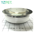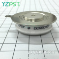


高DV/DT機能320A位相制御サイリスタ
$452-49 Piece/Pieces
$39≥50Piece/Pieces
| お支払い方法の種類: | L/C,T/T,Paypal |
| インコタームズ: | FOB,CFR,CIF |
| 輸送方法: | Ocean,Air |
| ポート: | Shanghai |

$452-49 Piece/Pieces
$39≥50Piece/Pieces
| お支払い方法の種類: | L/C,T/T,Paypal |
| インコタームズ: | FOB,CFR,CIF |
| 輸送方法: | Ocean,Air |
| ポート: | Shanghai |
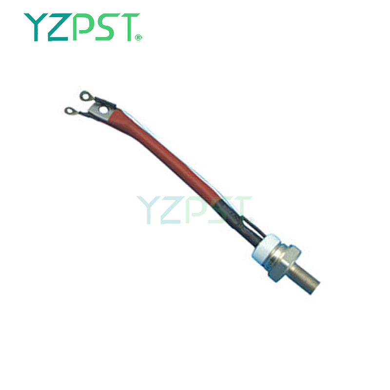
モデル: YZPST-T171-320-10
ブランド: yzpst
供給タイプ: 元のメーカー
参考資料: 写真, その他
構成: アレイ
現在の内訳: 適用できません
動作温度: -40°C〜125°C
SCRタイプ: 敏感な門
構造: シングル
電圧オン: 適用できません
電圧ゲートトリガー(Vgt)(最大): 適用できません
電流出力(最大): 適用できません
ITRMS: 502A
ITSM: 7kA
IH: 300mA
| 販売単位 | : | Piece/Pieces |
| ダウンロード | : |
|

位相制御サイリスタ
YZPST-T171-320-10
特徴
ゲート構成の中心を増幅します
圧縮結合カプセル化
高DV/DT機能
スタッドタイプ、スレッドインチまたはメトリック
代表的なアプリケーション
中電源スイッチング
DC電源
最大評価と特性
|
Symbol |
Parameter |
Values |
Units |
Test Conditions |
|
|
ON-STATE |
|
|
|
||
|
ITAV |
Mean on-state current |
320 |
A |
Sinewave,180° conduction,Tc=84oC |
|
|
ITRMS |
RMS value of on-state current |
502 |
A |
Nominal value |
|
|
ITSM |
Peak one cycle surge (non repetitive) current |
7 |
kA |
10.0 msec (50Hz), sinusoidal wave- shape, 180o conduction, Tj = 125 oC |
|
|
I2t |
I square t |
240 |
KA2s |
8.3 msec and 10.0 msec |
|
|
IL |
Latching current |
700 |
mA |
VD = 24 V; RL= 12 ohms |
|
|
IH |
Holding current |
300 |
mA |
VD = 24 V; I = 2.5 A |
|
|
VTM |
Peak on-state voltage |
1.6 |
V |
ITM = 1005 A |
|
|
di/dt |
Critical rate of rise of on-state current |
non-repetitive |
1000 |
A/ms |
Gate drive 20V, 20Ω, tr≤1μs, Tj=Tjmax, anode voltage≤80% VDRM |
|
repetitive |
- |
||||
|
BLOCKING |
|
|
|
||
|
VDRM VRRM |
Repetitive peak off state voltage Repetitive peak reverse voltage |
1000 |
V |
|
|
|
VDSM VRSM |
Non repetitive peak off state voltage Non repetitive peak reverse voltage |
1100 |
V |
|
|
|
IDRM IRRM |
Repetitive peak off state current Repetitive peak reverse current |
70 |
mA |
Tj = 100 oC ,VRRM VDRM applied |
|
|
dV/dt |
Critical rate of voltage rise |
500 |
V/ms |
TJ=TJmax, linear to 80% rated VDRM |
|
|
TRIGGEING |
|
|
|
||
|
PG(AV) |
Average gate power dissipation |
3 |
W |
|
|
|
PGM |
Peak gate power dissipation |
- |
W |
|
|
|
IGM |
Peak gate current |
6 |
A |
|
|
|
IGT |
Gate trigger current |
250 |
mA |
TC = 25 oC |
|
|
VGT |
Gate trigger voltage |
2.5 |
V |
TC = 25 oC |
|
|
VGD |
Gate non-trigger voltage |
0.6 |
V |
Tj = 125 oC |
|
|
VT0 |
|
1.006 |
V |
Tj = 125 oC |
|
|
rT |
|
0612 |
mΩ |
|
|
|
SWITCHING |
|
|
|
||
|
tq |
Turn-off time |
125 |
ms |
ITM=320A, TJ=TJmax, di/dt=10A/μs, VR=100V,dv/dt=50V/μs, Gate 0V 100Ω, tp=500μs |
|
|
td |
Delay time |
- |
Gate current A, di/dt=40A/μs, Vd=0.67%VDRM, TJ=25 oC |
||
サーマルおよびメカニカル
|
Symbol |
Parameter |
Values |
Units |
Test Conditions |
|
Tj |
Operating temperature |
-40~125 |
oC |
|
|
Tstg |
Storage temperature |
-40~125 |
oC |
|
|
R th (j-c) |
Thermal resistance - junction to case |
0.085 |
oC/W |
DC operation ,Single sided cooled |
|
R th (c-s) |
Thermal resistance - case to sink |
- |
oC/W |
Single sided cooled |
|
P |
Mounting force |
- |
Nm |
± 10 % |
|
W |
Weight |
440 |
g |
about |
概要


電話番号: 86-514-87782298
Whatsapp: +8613805278321
住所: 3rd Floor, Weiheng Building No.20 B Area, Yangzhou, Jiangsu China
ウェブサイト: https://jp.yzpst.com


Privacy statement: Your privacy is very important to Us. Our company promises not to disclose your personal information to any external company with out your explicit permission.
Fill in more information so that we can get in touch with you faster
Privacy statement: Your privacy is very important to Us. Our company promises not to disclose your personal information to any external company with out your explicit permission.