

85A電子シガーライターMosfet Load 85N03
$0.299≥1000Piece/Pieces
| お支払い方法の種類: | L/C,T/T,Paypal |
| インコタームズ: | FOB,CFR,CIF |
| 最小注文数: | 1000 Piece/Pieces |
| 輸送方法: | Ocean,Air |
| ポート: | Shanghai |

$0.299≥1000Piece/Pieces
| お支払い方法の種類: | L/C,T/T,Paypal |
| インコタームズ: | FOB,CFR,CIF |
| 最小注文数: | 1000 Piece/Pieces |
| 輸送方法: | Ocean,Air |
| ポート: | Shanghai |
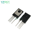
モデル: YZPST-85N03
ブランド: YZPST
| 販売単位 | : | Piece/Pieces |
| パッケージ型式 | : | 1.帯電防止包装2.カートン箱3.プラスチック保護包装 |
電子タバコ用ライターMosfet
YZPST-85N03
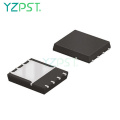
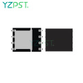
85A電子シガレットライターMosfetロードスイッチMosfet 85N03
|
VDSS30V RDS(ON) 2.3mΩ(max.)@ VGS=10V RDS(ON) 3.0mΩ(max.)@ VGS=4.5V ID 85A |
|
|
Description |
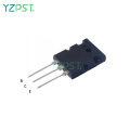
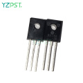
DFN5X6-8L |
|
YZPST85N03 uses advanced Trench technology and designs to provide excellent RDS(ON) with low gate charge. This device is suitable for use in PWM, load switching and general purpose applications. |
|
|
Applications |
Features |
|
■ Lithium-Ion Secondary Batteries ■ Load Switch ■ DC-DC converters and Off-line UPS |
■ Low On-Resistance ■ Low Input Capacitance ■ Low Miller Charge ■ Low Input / Output Leakage |
|
Absolute Maximum Ratings (TA=25°C unless otherwise noted) |
|||
|
Parameter |
Symbol |
Value |
Unit |
|
Drain-Source Voltage |
VDSS |
30V |
V |
|
Gate-Source Voltage |
VGSS |
±20V |
V |
|
Drain Current-Continuous @ TC=25℃ NOTE 3 |
ID |
85 |
A |
|
Drain Current-Continuous @ TC=100℃ NOTE 3 |
68 |
A |
|
|
Drain Current-Pulsed NOTE 1 |
IDM |
320 |
A |
|
Avalanche Current, L=0.1mH |
IAS |
50 |
A |
|
Avalanche Energy, L=0.1mH |
EAS |
125 |
mJ |
|
Maximum Power Dissipation @ TC=25℃ |
PD |
60 |
W |
|
Maximum Power Dissipation @ TA=25℃ |
5.7 |
W |
|
|
Storage Temperature Range |
TSTG |
-50 to 150°C |
°C |
|
Operating Junction Temperature Range |
TJ |
-50 to 150°C |
°C |
|
Thermal Resistance Ratings |
||||||
|
Parameter |
Symbol |
Conditions |
Min. |
Typ. |
Max. |
Unit |
|
Maximum Junction-to-Ambient NOTE2 |
RθJA |
Steady State |
- |
- |
22 |
°C/W |
|
Maximum Junction-to-Case |
RθJC |
Steady State |
- |
- |
2.1 |
°C/W |
|
Electrical Characteristics(TJ=25°C unless otherwise noted) |
||||||
|
Parameter |
Symbol |
Conditions |
Min. |
Typ. |
Max. |
Unit |
|
OFF CHARACTERISTICS |
||||||
|
Drain-Source Breakdown Voltage |
BVDSS |
VGS=0V , IDS=250uA |
30 |
- |
- |
V |
|
Zero Gate Voltage Drain Current |
IDSS |
VDS=30V, VGS=0V |
- |
- |
1 |
uA |
|
Gate-Source Leakage Current |
IGSS |
VGS=±20V , VDS=0V |
- |
- |
±100 |
nA |
|
ON CHARACTERISTICS |
||||||
|
Gate Threshold Voltage |
VGS(TH) |
VGS=VDS, IDS=250uA |
1.2 |
- |
2.5 |
V |
|
Drain-Source On-Resistance |
RDS(ON) |
VGS=10V , IDS=16A |
- |
1.75 |
2.3 |
mΩ |
|
VGS=4.5V , IDS=16A |
- |
2.6 |
3.0 |
|||
|
DYNAMIC CHARACTERISTICS |
||||||
|
Input Capacitance |
Ciss |
VDS=10V, VGS=0V, f=1MHz |
- |
5910 |
- |
pF |
|
Output Capacitance |
Coss |
- |
725 |
- |
||
|
Reverse Transfer Capacitance |
Crss |
- |
537 |
- |
||
|
SWITCHING CHARACTERISTICS |
||||||
|
Turn-On Delay Time |
Td(on) |
VDS=15V, VGS=10V, ID=1A , RGEM=3.3Ω |
- |
20 |
- |
ns |
|
Rise Time |
tr |
- |
6.5 |
- |
||
|
Turn-Off Delay Time |
Td(off) |
- |
122 |
- |
||
|
Fall Time |
tf |
- |
15 |
- |
||
|
Total Gate Charge at 4.5V |
Qg |
VDS=15V, IDS=16A, VGS=10V |
- |
54 |
- |
nC |
|
Gate to Source Gate Charge |
Qgs |
- |
18 |
- |
||
|
Gate to Drain "Miller" Charge |
Qgd |
- |
20.5 |
- |
||
|
SWITCHING CHARACTERISTICS |
||||||
|
Drain-Source Diode Forward Voltage |
VSD |
VGS=0V, IS=4A |
- |
- |
1.3 |
V |
|
Body Diode Reverse Recovery Time |
trr |
If=10A, dl/dt=100A/μs, TJ=25°C |
- |
46 |
- |
ns |
|
Body Diode Reverse Recovery Charge |
Qrr |
- |
38 |
- |
nC |
|
ノート:
パルステスト:パルス幅≦300μs、デューティサイクル≦2%。
2.RΘJAは、接合部 - ケース間およびケース - 周囲間の熱抵抗の合計です。ここで、ケースの熱基準は、ドレインピンの半田付け面と定義されます。 RΘJCは設計によって保証されていますが、RΘCAはユーザのボード設計によって決定されます。下記のRΘJAは、FR-4でのシングルデバイス操作用です。
まだ空気。
3.最大電流定格はパッケージによって制限されています。
")
")
")
")


電話番号: 86-514-87782298
Whatsapp: +8613805278321
住所: 3rd Floor, Weiheng Building No.20 B Area, Yangzhou, Jiangsu China
ウェブサイト: https://jp.yzpst.com


Privacy statement: Your privacy is very important to Us. Our company promises not to disclose your personal information to any external company with out your explicit permission.
Fill in more information so that we can get in touch with you faster
Privacy statement: Your privacy is very important to Us. Our company promises not to disclose your personal information to any external company with out your explicit permission.