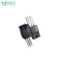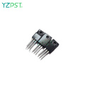

1500V N-Channel Power MOSFET
$2.15100-999 Piece/Pieces
$1.85≥1000Piece/Pieces
| お支払い方法の種類: | L/C,T/T,Paypal |
| インコタームズ: | FOB,CFR,CIF |
| 輸送方法: | Ocean,Air |
| ポート: | SHANGHAI |

$2.15100-999 Piece/Pieces
$1.85≥1000Piece/Pieces
| お支払い方法の種類: | L/C,T/T,Paypal |
| インコタームズ: | FOB,CFR,CIF |
| 輸送方法: | Ocean,Air |
| ポート: | SHANGHAI |
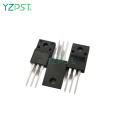
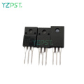
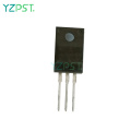
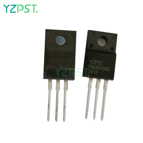
モデル: YZPST-FM3N150C
ブランド: yzpst
原産地: 中国
Vdss: 1500V
ID Continuous (Tc = 25 °C ): 1.8A
ID Continuous ( Tc = 100 °C ): 1.2A
Idm: 12A
Vgss: ±30V
EAS: 225mJ
Dv/dt: 5V/ns
| 販売単位 | : | Piece/Pieces |
| パッケージ型式 | : | 1.抗血圧剤パッケージ2.カートンボックス3.プラスチック保護パッケージング |
| ダウンロード | : |
|
1500V N-Channel Mosfet
YZPST-FM3N150C
概要
このパワーMOSFETは、高度な自己整合平面技術を使用して生産されます。この高度なテクノロジーは、州内抵抗を最小限に抑え、優れたスイッチングパフォーマンスを提供し、雪崩および整流モードで高エネルギーパルスに耐えるように特に調整されています。
これらのデバイスは、システムの小型化とより高い効率のために、さまざまな電源スイッチング回路で使用できます。
特徴
3a、1500v、rds(on)typ。 = 5q@vgs = 10 V ld = 1.5a
低ゲートチャージ(典型的な9.3NC)
低ゲートチャージ(典型的な2.4pf)
高速スイッチング
100%雪崩をテストしました
特に明記しない限り、絶対最大評価TC = 25°C
| Symbol | Parameter | JFFM3N150C | Units | |
| Vdss | Drain - Source Voltage | 1500 | V | |
| Id | Drain Current | Continuous (Tc = 25 °C ) | 1.8 | A |
| Continuous ( Tc = 100 °C ) | 1.2 | A | ||
| Idm | Drain Current - Pulsed ( Note 1) | 12 | A | |
| Vgss | Gate - Source Voltage | ±30 | V | |
| EAS | Single Pulsed Avalanche Energy ( Note 2 ) | 225 | mJ | |
| dv/dt | Peak Diode Recovery dv/dt ( Note 3 ) | 5 | V/ns | |
| Pd | Power Dissipation (Tc = 25 °C ) | 30 | W | |
| Tj,Tstg | Operating and Storage Temperature Range | -55 to +150 | °C | |
| Tl | Maximum lead temperature for soldering purposes | 300 | °C | |
| 1/8 frome case for 5 seconds | ||||
熱特性
| Symbol | Parameter | JFFM3N150C | Units |
| Raic | Thermal Resistance, Junction-to-Case | 4.1 | °C/W |
| Rqja | Thermal Resistance, Junction-to-Ambient | 62.5 | °c/w |
特に明記しない限り、電気特性TC = 25°C
| Symbol | Parameter | Test Conditions | Min | Typ | Max | Units |
| Off Characteristics | ||||||
| BVdss | Drain - Source Breakdown Voltage | Vgs = 0 V, Id =250 uA | 1500 | V | ||
| / BVdss/ | Breakdown Voltage Temperature Coefficient | Id = 250 uA, Referenced to | -- | 1.3 | -- | v/°c |
| Tj | 25 °C | |||||
| Zero Gate Voltage Drain Current | Vds = 1500 V, Vgs = 0 V | 25 | uA | |||
| Idss | Vds = 1200 V, Tc = 125 °C | -- | -- | 500 | uA | |
| Igssf | Gate-Body Leakage Current, Forward | Vgs = 30 V, Vgs = 0 V | — | — | 100 | nA |
| Igssr | Gate-Body Leakage Current, Reverse | Vgs = -30 V, Vgs = 0 V | — | — | -100 | nA |
| On Characteristics | ||||||
| VGS(th) | Gate Threshold Voltage | Vds = Vgs, Id = 250 uA | 3 | — | 5 | V |
| RDS(on) | Static Drain-Source on-Resista nee | Vgs = 10 V, Id= 1.5A | — | 5 | 8 | Q |
| gFS | Forward Transconductance | Vds = 30 V, Id= 1.5 A ( Note | -- | 4.5 | -- | S |
| 4) | ||||||
| Dynamic Characteristics | ||||||
| Ciss | Input Capacitance | Vds = 25 V, Vgs = 0 V, f = | — | 1938 | — | pF |
| Coss | Output Capacitance | 1.0 MHz | — | 104 | — | pF |
| Crss | Reverse Transfer Capacitance | — | 2.4 | — | pF | |
| Rg | Gate resistance | F= 1.0 MHz | 3.5 | Q | ||
| Switching Characteristics | ||||||
| td(on) | Turn-On Delay Time | 34 | ns | |||
| tr | Turn-On Rise Time | Vds = 750 V, Id=3.0A/ Rg = | 17 | ns | ||
| td(off) | Turn-Off Delay Time | 100 , Vgs = 10 V (Note 4,5) | 56 | ns | ||
| tf | Turn-Off Fall Time | 27 | ns | |||
| Qe | Total Gate Charge | Vds = 750 V, Id =3.0 A Vgs = | 9.3 | nC | ||
| Qgs | Gate-Source Charge | 10 V (Note 4,5) | 15 | nC | ||
| Qgd | Gate-Drain Charge | 5.3 | nC | |||
| Drain - Source Diode Characteristics and Maximum Ratings | ||||||
| Is | Maximum Continuous Drain-Source Diode Forward Current | 3 | A | |||
| Ism | Maximum Pulsed Drain-Source Diode Forward Current | 12 | A | |||
| Vsd | Drain-Source Diode Forward Voltage | Vgs = 0 V, Is = 3.0 A | 1.5 | V | ||
| trr | Reverse Recovery Time | Vgs = 0 V, Is = 3.0 A | 302 | ns | ||
| Qrr | Reverse Recovery Charge | dlF/dt = 100 A/us ( Note | -- | 10 | -- | uC |
| 4) | ||||||
ノート:
1.繰り返し評価:パルス幅が最大接合温度によって制限されています
2. l = lo.omh、ias = 6.7a、rg = 25q、starttj = 25°C
3.ISD <3.0A Z DI/DT <LOOA/US、VDD <BVDSS、開始TJ = 25°C
4.パルステスト:パルス幅<3oous Zデューティサイクル< 2%
5.本質的に動作温度とは無関係です


電話番号: 86-514-87782298
Whatsapp: +8613805278321
住所: 3rd Floor, Weiheng Building No.20 B Area, Yangzhou, Jiangsu China
ウェブサイト: https://jp.yzpst.com


Privacy statement: Your privacy is very important to Us. Our company promises not to disclose your personal information to any external company with out your explicit permission.
Fill in more information so that we can get in touch with you faster
Privacy statement: Your privacy is very important to Us. Our company promises not to disclose your personal information to any external company with out your explicit permission.