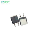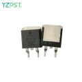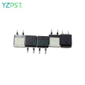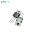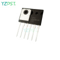
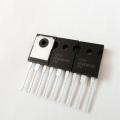
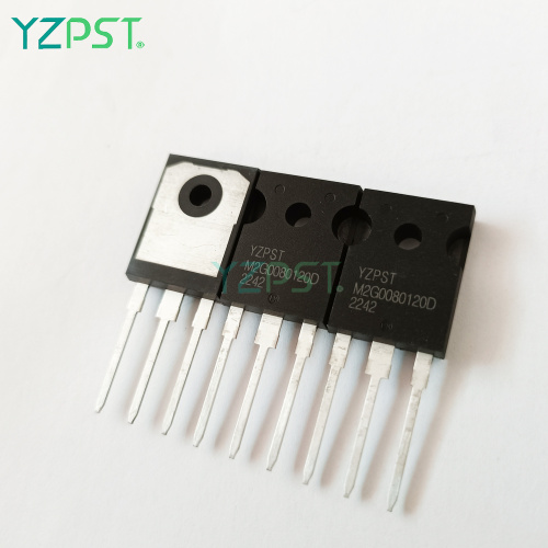

1200V N-Channel Silicon Carbide Power MOSFET SIC MOSFET
$10100-999 Piece/Pieces
$6.5≥1000Piece/Pieces
| お支払い方法の種類: | L/C,T/T,Paypal |
| インコタームズ: | FOB,CFR,CIF |
| 輸送方法: | Ocean,Air |
| ポート: | SHANGHAI |

$10100-999 Piece/Pieces
$6.5≥1000Piece/Pieces
| お支払い方法の種類: | L/C,T/T,Paypal |
| インコタームズ: | FOB,CFR,CIF |
| 輸送方法: | Ocean,Air |
| ポート: | SHANGHAI |
モデル: YZPST-M2G0080120D
ブランド: yzpst
VDSmax: 1200V
Id: 42A
Pd: 208W
VGS,op: -5/+20V
VGSmax: -10/+25V
| 販売単位 | : | Piece/Pieces |
| パッケージ型式 | : | 1.抗血小ロスタチックパッケージ2.カートンボックス3.プラスチック保護パッケージング |
| ダウンロード | : |
|

M2G0080120D
1200V N-Channel Silicon Carbide Power MOSFET SIC MOSFET
特徴
•個別のドライバーソースピンを備えた最適化されたパッケージ
•低い抵抗の高いブロッキング電圧
•低容量による高速スイッチング
•低い逆回復を伴う高速固有のダイオード(QRR)
•平行に簡単です
• RoHS対応
利点
•より高いシステム効率
•冷却要件を削減します
•電力密度の増加
•より高い周波数を有効にします
•ゲートリングを最小化します
•システムの複雑さとコストの削減
アプリケーション
•スイッチモード電源
• DC/DCコンバーター
•ソーラーインバーター
•バッテリー充電器
•モータードライブ

最大評価(TC = 25°C特に指定がない限り)
| Symbol | Parameter | Value | Unit | Test Conditions | Note |
| f^DSmax | Drain-Source Breakdown Voltage | 1200 | V | 海=0 V, /d=100 卩A | |
| Id | Continuous Drain Current | 42 | A | 4s=20 V Tc=25 °C | Fig. 18 |
| Pd | Power Dissipation | 208 | W | *=25 °C | Fig. 19 |
| FgS,op | Recommend Gate Source Voltage | -0.25 | V | ||
| J^Smax | Maximum Gate Source Voltage | -0.4 | V | AC (f>lHz) | Note 1 |
| Tj, Tstg | Operating Junction and Storage Temperature Range | -55 to | °C | ||
| 175 | |||||
| 7l | Soldering Temperature | 260 | °C |
電気的特性
| Symbol | Parameter | Min. | Typ. | Max. | Unit | Test Conditions | Note |
| Static | |||||||
| BVds | Drain-Source Breakdown Voltage | 1200 | - | - | V | 4s=0 V, Zd=100 卩A | |
| A)ss | Zero Gate Voltage Drain Current | — | 11 | 100 | 丹s=1200 V Pgs=0 V | ||
| Igss | Gate-Source Leakage | — | 10 | 250 | nA | 4s=20 V | |
| FGS(th) | Gate-Source Threshold Voltage | 2 | — | 4 | V | Id=5 mA, | Fig. 11 |
| &DS(on) | Drain-Source On-Resistance | — | 78 | 100 | mQ | 国=20 V, Zd=20 A | Fig. 6 |
| Dynamic | |||||||
| Ciss | Input Capacitance | — | 1128 | PF | 4s=0 V,比s=1000 V | Fig. 17 | |
| C^oss | Output Capacitance | — | 86 | f^l.OMHz,瓜=25 mV | |||
| Crss | Reverse Transfer Capacitance | — | 5 | ||||
| Eoss | Coss Stored Energy | - | 44 | 卩J | Fig. 16 | ||
| Qs | Total Gate Charge | — | 52 | nC | moo V | Fig. 12 | |
| figs | Gate-Source Charge | - | 17 | 血=20 A | |||
| Qgd | Gate-Drain Charge | - | 15 | Fgs=-5/+20 V | |||
| td(cn) | Turn-on Delay Time | — | 41 | ns | 丹 s=800 V | ||
| tr | Turn-on Rise Time | - | 21 | Fgs=-5/+20 V | |||
| Turn-off Delay Time | — | 48 | Id=20A | ||||
| tf | Turn-off Fall Time | — | 16 | Ro(ext)=2.5 Q | |||
| RG(int) | Internal Gate Resistance | - | 4 | n | E.O MHz, Vac=25 mV | ||
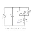
回路回路図をテストします

SIC MOSFET


電話番号: 86-514-87782298
Whatsapp: +8613805278321
住所: 3rd Floor, Weiheng Building No.20 B Area, Yangzhou, Jiangsu China
ウェブサイト: https://jp.yzpst.com


Privacy statement: Your privacy is very important to Us. Our company promises not to disclose your personal information to any external company with out your explicit permission.
Fill in more information so that we can get in touch with you faster
Privacy statement: Your privacy is very important to Us. Our company promises not to disclose your personal information to any external company with out your explicit permission.