
高速スイッチング800V N-Channel Power MOSFET
$5510-199 Piece/Pieces
$45≥200Piece/Pieces
| お支払い方法の種類: | L/C,T/T,Paypal |
| インコタームズ: | FOB,CFR,CIF |
| 輸送方法: | Ocean,Air |
| ポート: | SHANGHAI |

$5510-199 Piece/Pieces
$45≥200Piece/Pieces
| お支払い方法の種類: | L/C,T/T,Paypal |
| インコタームズ: | FOB,CFR,CIF |
| 輸送方法: | Ocean,Air |
| ポート: | SHANGHAI |
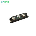
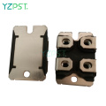
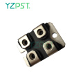
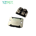
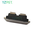
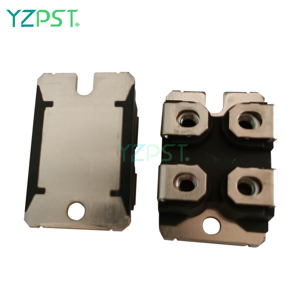
モデル: YZPST-SP50N80FX
ブランド: yzpst
供給タイプ: 元のメーカー, ODM, エージェンシー, 小売業者
参考資料: データシート, 写真
構成: アレイ
現在の内訳: 適用できません
電流保持(Ih)(最大): 適用できません
電流オフ状態(最大): 適用できません
SCR番号、ダイオード: 適用できません
動作温度: -55°C〜150°C(TJ)
SCRタイプ: 標準リカバリ
構造: 適用できません
電圧オン: 適用できません
電圧ゲートトリガー(Vgt)(最大): 適用できません
電流出力(最大): 適用できません
VDSS: 800V
ID: 50A
IDM: 200A
VGSS: ±30V
EAS: 4500mJ
EAR: 60mJ
P: 690w
TJ, Tstg: -55~+150ºC
| 販売単位 | : | Piece/Pieces |
| 写真の例 | : |

|
| ダウンロード | : |
|

800V N-Channel Power MOSFET
YZPST-SP50N80FX
特徴
高速スイッチング
100%雪崩をテストしました
DV/DT機能の改善
アプリケーション
スイッチモード電源(SMPS)
無停電電源(UPS)
力率補正(PFC) 
|
Device Ordering Marking Packing Information |
|||
|
Ordering Number |
Package |
Marking |
Packing |
|
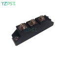
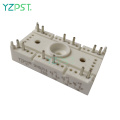
SP50N80FX |
SOT-227 |
SP50N80FX |
Tube |
|
Absolute Maximum Ratings TC = 25ºC, unless otherwise noted |
|||
|
Parameter |
Symbol |
Value |
Unit |
|
Drain-Source Voltage (VGS = 0V) |
VDSS |
800 |
V |
|
Continuous Drain Current |
ID |
50 |
A |
|
Pulsed Drain Current (note1) |
IDM |
200 |
A |
|
Gate-Source Voltage |
VGSS |
±30 |
V |
|
Single Pulse Avalanche Energy (note2) |
EAS |
4500 |
mJ |
|
Repetitive Avalanche Energy (note1) |
EAR |
60 |
mJ |
|
Power Dissipation (TC = 25ºC) |
PD |
690 |
W |
|
Operating Junction and Storage Temperature Range |
TJ, Tstg |
-55~+150 |
ºC |
|
Caution: Stresses greater than those listed in the “Absolute Maximum Ratings” may cause permanent damage to the device. |
|||
|
Thermal Resistance |
|||
|
Parameter |
Symbol |
Value |
Unit |
|
Thermal Resistance, Junction-to-Case |
RthJC |
0.18 |
ºC/W |
|
Thermal Resistance, Junction-to-Ambient |
RthJA |
40 |
|
|
Specifications TJ = 25ºC, unless otherwise noted |
||||||
|
Parameter |
Symbol |
Test Conditions |
Value |
Unit |
||
|
Min. |
Typ. |
Max. |
||||
|
Static |
||||||
|
Drain-Source Breakdown Voltage |
V(BR)DSS |
VGS = 0V, ID = 250µA |
800 |
-- |
-- |
V |
|
Zero Gate Voltage Drain Current |
IDSS |
VDS =800, VGS = 0V, TJ = 25ºC |
-- |
-- |
1.0 |
μA |
|
Gate-Source Leakage |
IGSS |
VGS = ±30V |
-- |
-- |
±100 |
nA |
|
Gate-Source Threshold Voltage |
VGS(th) |
IDS = 250µA |
2.5 |
-- |
4.5 |
V |
|
Drain-Source On-Resistance (Note3) |
RDS(on) |
VGS = 10V, ID = 25A |
-- |
120 |
130 |
mΩ |
|
Dynamic |
||||||
|
Input Capacitance |
Ciss |
VGS = 0V, VDS = 25V, f = 1.0MHz |
-- |
14600 |
-- |
pF |
|
Output Capacitance |
Coss |
-- |
1300 |
-- |
||
|
Reverse Transfer Capacitance |
Crss |
-- |
66 |
-- |
||
|
Total Gate Charge |
Qg |
VDD =400V, ID =50A, VGS = 10V |
-- |
360 |
-- |
nC |
|
Gate-Source Charge |
Qgs |
-- |
80 |
-- |
||
|
Gate-Drain Charge |
Qgd |
-- |
120 |
-- |
||
|
Turn-on Delay Time |
td(on) |
VDD = 400V, ID =50A, RG = 10 Ω |
-- |
110 |
-- |
ns |
|
Turn-on Rise Time |
tr |
-- |
200 |
-- |
||
|
Turn-off Delay Time |
td(off) |
-- |
160 |
-- |
||
|
Turn-off Fall Time |
tf |
-- |
185 |
-- |
||
|
Drain-Source Body Diode Characteristics |
||||||
|
Continuous Body Diode Current |
IS |
TC = 25 ºC |
-- |
-- |
50 |
A |
|
Pulsed Diode Forward Current |
ISM |
-- |
-- |
400 |
||
|
Body Diode Voltage |
VSD |
TJ = 25ºC, ISD = 25A, VGS = 0V |
-- |
-- |
1.4 |
V |
|
Reverse Recovery Time |
trr |
VGS = 0V,IS = 50A, diF/dt =100A /μs |
-- |
520 |
-- |
ns |
|
Reverse Recovery Charge |
Qrr |
-- |
5.0 |
-- |
μC |
|
ノート
1。繰り返し評価:パルス幅が最大接合温度によって制限されています
2。 v dd = 50V、r g =25Ω、開始t j = 25ºC
パルステスト:パルス幅≤300μs、デューティサイクル≤1%


電話番号: 86-514-87782298
Whatsapp: +8613805278321
住所: 3rd Floor, Weiheng Building No.20 B Area, Yangzhou, Jiangsu China
ウェブサイト: https://jp.yzpst.com


Privacy statement: Your privacy is very important to Us. Our company promises not to disclose your personal information to any external company with out your explicit permission.
Fill in more information so that we can get in touch with you faster
Privacy statement: Your privacy is very important to Us. Our company promises not to disclose your personal information to any external company with out your explicit permission.