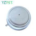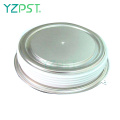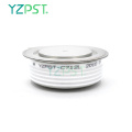
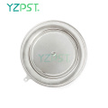
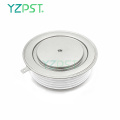
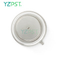

C712Lサイリスタ電源コントローラKT55CT
$801-99 Piece/Pieces
$40≥100Piece/Pieces
| お支払い方法の種類: | L/C,T/T,Paypal |
| インコタームズ: | FOB,CFR,CIF |
| 最小注文数: | 1 Piece/Pieces |
| 輸送方法: | Ocean,Air |
| ポート: | Shanghai |

$801-99 Piece/Pieces
$40≥100Piece/Pieces
| お支払い方法の種類: | L/C,T/T,Paypal |
| インコタームズ: | FOB,CFR,CIF |
| 最小注文数: | 1 Piece/Pieces |
| 輸送方法: | Ocean,Air |
| ポート: | Shanghai |
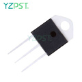
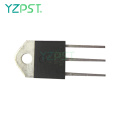
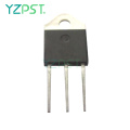
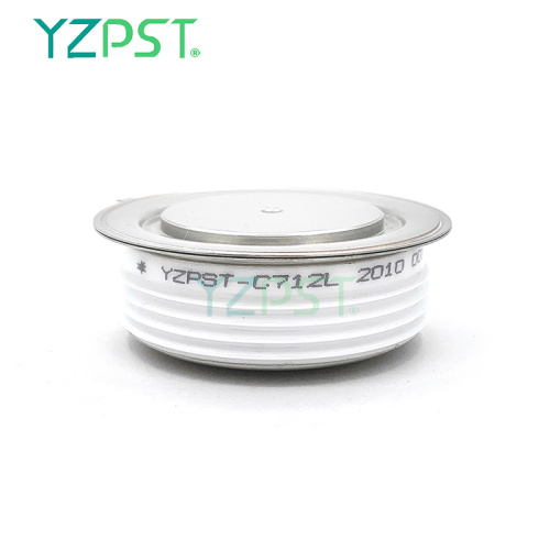
モデル: YZPST-C712L
ブランド: YZPST

インバーターおよびチョッパーアプリケーション向けの高出力サイリスタ
YZPST-C712L
特徴:
。すべての拡散構造
。センター増幅ゲート構成
。最大2100ボルトのブロッキング機能
。保証された最大ターンオフ時間
。高いdV / dt機能
。圧力組立装置
ブロッキング-オフ状態
|
VRRM (1) |
VDRM (1) |
VRSM (1) |
|
2000 |
2000 |
2100 |
V RRM =繰り返しピーク逆電圧
V DRM =繰り返しピークオフ状態電圧
V RSM =非繰り返しピーク逆電圧(2)
|
Repetitive peak reverse leakage and off state leakage |
IRRM / IDRM
|
20 mA 90 mA (3) |
|
Critical rate of voltage rise |
dV/dt (4) |
800 V/msec |
ノート:
すべての定格は、Tj = 25 o Cに対して指定されています。
特に明記されていません。
(1)すべての電圧定格は、適用される
50Hz / 60zHzの正弦波形
温度範囲-40〜+125 o C
(2)10ミリ秒。マックス。パルス幅
(3)Tj = 125 o Cの最大値。
(4)線形および指数関数の最小値
80%定格のV DRMへの波形。ゲートが開いています。
Tj = 125 oC 。
(5)非反復値。
(6)di / dtの値は、
EIA / NIMA標準RS-397付き、セクション
5-2-2-6。定義された値はさらに追加されます
スナバ回路から得られるものに
0.2 mFコンデンサと20オーム
下のスリスタと並列の抵抗
テスト。
伝導-状態
|
Parameter |
Symbol |
Min. |
Max. |
Typ. |
Units |
Conditions |
|
Average value of on-state current |
IT(AV) |
|
1185 |
|
A |
Sinewave,180o conduction,Tc=80oC |
|
RMS value of on-state current |
ITRMS |
|
1700 |
|
A |
Nominal value |
|
Peak one cPSTCle surge (non repetitive) current |
ITSM |
|
-
18500 |
|
A
A |
8.3 msec (60Hz), sinusoidal wave- shape, 180o conduction, Tj = 125 oC 10.0 msec (50Hz), sinusoidal wave- shape, 180o conduction, Tj = 125 oC |
|
I square t |
I2t |
|
1.66x10⁶ |
|
A2s |
8.3 msec and 10.0 msec |
|
Latching current |
IL |
|
- |
|
mA |
VD = 24 V; RL= 12 ohms |
|
Holding current |
IH |
|
- |
|
mA |
VD = 24 V; I = 2.5 A |
|
Peak on-state voltage |
VTM |
|
1.45 |
|
V |
ITM = 1000 A; Duty Cycle £ 0.01%; Tj =1 25 oC |
|
Critical rate of rise of on-state current (5, 6) |
di/dt |
|
800 |
|
A/ms |
Switching from VDRM £ 1000 V, non-repetitive |
|
Critical rate of rise of on-state current (6) |
di/dt |
|
200 |
|
A/ms |
Switching from VDRM £ 1000 V |
ゲーティング
|
Parameter |
Symbol |
Min. |
Max. |
Typ. |
Units |
Conditions |
|
Peak gate power dissipation |
PGM |
|
100 |
|
W |
tp = 40 us |
|
Average gate power dissipation |
PG(AV) |
|
5 |
|
W |
|
|
Peak gate current |
IGM |
|
- |
|
A |
|
|
Gate current required to trigger all units |
IGT |
|
- 120 - |
|
mA mA mA |
VD = 6 V;RL = 3 ohms;Tj = -40 oC VD = 6 V;RL = 3 ohms;Tj = +25 oC VD = 6 V;RL = 3 ohms;Tj = +125oC |
|
Gate voltage required to trigger all units
|
VGT |
|
- 3.0 -
|
|
V V V |
VD = 6 V;RL = 3 ohms;Tj = -40 oC VD = 6 V;RL = 3 ohms;Tj = 0-125oC VD = Rated VDRM; RL = 1000 ohms; Tj = + 125 oC |
|
Peak negative voltage |
VGRM |
|
20 |
|
V |
|
動的
|
Parameter |
Symbol |
Min. |
Max. |
Typ. |
Units |
Conditions |
|
Delay time |
td |
|
- |
0.7 |
ms |
ITM = 50 A; VD = Rated VDRM Gate pulse: VG = 20 V; RG = 20 ohms; tr = 0.1 ms; tp = 20 ms |
|
Turn-off time (with VR = -50 V) |
tq |
|
40 |
- |
ms |
ITM = 1000 A; di/dt = 25 A/ms; VR ³ -50 V; Re-applied dV/dt = 20 V/ms linear to 80% VDRM; VG = 0; Tj = 125 oC; Duty cPSTCle ³ 0.01% |
|
Reverse recovery charge |
Qrr |
|
* |
|
mC |
ITM = 1000 A; di/dt = 25 A/ms; VR ³ -50 V |
熱的および機械的特性と評価
|
Parameter |
Symbol |
Min. |
Max. |
Typ. |
Units |
Conditions |
|
Operating temperature |
Tj |
-40 |
+125 |
|
oC |
|
|
Storage temperature |
Tstg |
-40 |
+125 |
|
oC |
|
|
Thermal resistance - junction to case |
RQ (j-c) |
|
0.023 - |
|
oC/W |
Double sided cooled Single sided cooled |
|
Thermal resistamce - case to sink |
RQ (c-s) |
|
0.0075 - |
|
oC/W |
Double sided cooled * Single sided cooled * |
|
Mounting force |
P |
22.2 |
26.6 |
|
kN |
|
|
Weight |
W |
|
|
- |
g |
About |


電話番号: 86-514-87782298
Whatsapp: +8613805278321
住所: 3rd Floor, Weiheng Building No.20 B Area, Yangzhou, Jiangsu China
ウェブサイト: https://jp.yzpst.com


Privacy statement: Your privacy is very important to Us. Our company promises not to disclose your personal information to any external company with out your explicit permission.
Fill in more information so that we can get in touch with you faster
Privacy statement: Your privacy is very important to Us. Our company promises not to disclose your personal information to any external company with out your explicit permission.