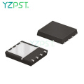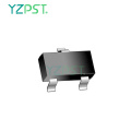

パワーMOSFET smd 110v STC2326
最新の価格を取得する| お支払い方法の種類: | L/C,T/T,Paypal |
| インコタームズ: | FOB,CFR,CIF |
| 輸送方法: | Ocean,Air |
| ポート: | SHANGHAI |

| お支払い方法の種類: | L/C,T/T,Paypal |
| インコタームズ: | FOB,CFR,CIF |
| 輸送方法: | Ocean,Air |
| ポート: | SHANGHAI |
モデル: YZPST-STC2326
ブランド: YZPST
B TA30シリーズトライアック
YZPST-STC2326
DESCRIPTION
STC2326は、超高密度DMOSトレンチ技術を使用して製造されたNチャネル・ロジック・エンハンスメント・モードのパワー電界効果トランジスタです。 STC2326は、同期または従来のスイッチングPWMコントローラを使用してDC / DCコンバータの総合効率を改善するように設計されています。低ゲート電荷、低RDS(ON)、高速スイッチング速度に最適化されています。
アプリケーション
電源システム
DC / DCコンバータ
ロードスイッチ
特徴
110V / 3A、RDS(ON)=310mΩ@ VGS = 10V
非常に低いRDS(ON)のための高密度セル設計
優れたオン抵抗と最大DC 電流能力
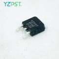
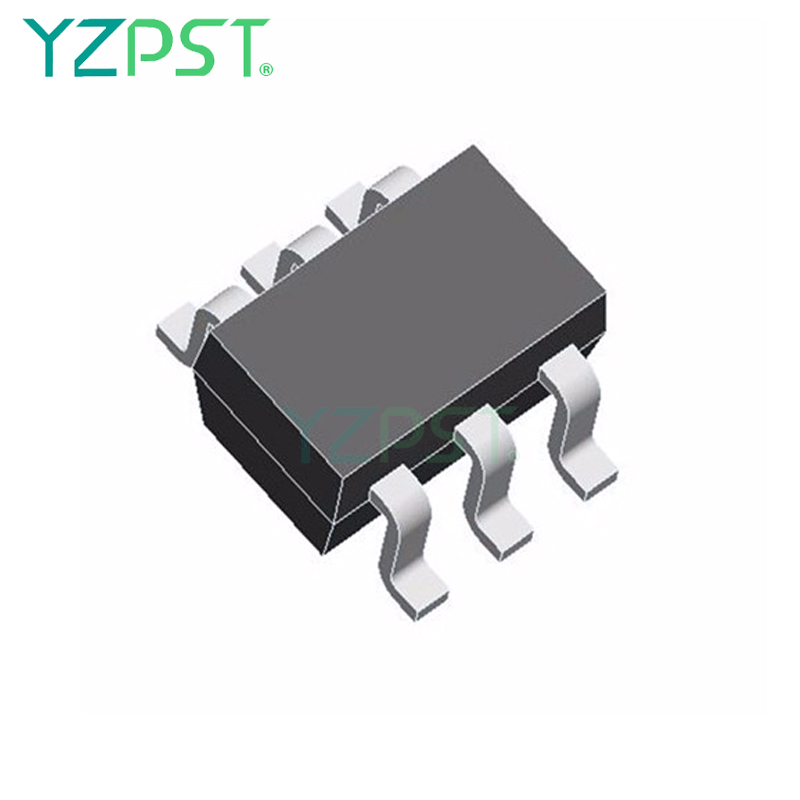
SOT-23-6Lパッケージデザイン
ピン配置(SOT-23-6L)
")
|
Pin |
Symbol |
Description |
|
1 |
D |
Drain |
|
2 |
D |
Drain |
|
3 |
G |
Gate |
|
4 |
S |
Source |
|
5 |
D |
Drain |
|
6 |
D |
Drain |
O RDER ING IN F O R M A T I O N
|
Part Number |
Package |
Part Marking |
|
SPN2326S26RGB |
SOT-23-6L |
26YW |
A B SOU L T E MA X I M U M R A T IN G S ( T A = 25℃ U n l e s s o t h e r w i s e n o t e d )
|
Parameter |
Symbol |
Typical |
Unit |
|
|
Drain-Source Voltage |
VDSS |
110 |
V |
|
|
Gate –Source Voltage |
VGSS |
±20 |
V |
|
|
Continuous Drain Current(TJ=150℃) |
TA=25℃ |
ID |
3.0 |
A |
|
TA=70℃ |
2.0 |
|||
|
Pulsed Drain Current |
IDM |
10 |
A |
|
|
Power Dissipation |
TA=25℃ |
PD |
2.0 |
W |
|
TA=70℃ |
1.3 |
|||
|
Operating Junction Temperature |
TJ |
-55/150 |
℃ |
|
|
Storage Temperature Range |
TSTG |
-55/150 |
℃ |
|
|
Thermal Resistance-Junction to Ambient |
RθJA |
62.5 |
℃/W |
|
|
Parameter |
Symbol |
Conditions |
Min. |
Typ |
Max. |
Unit |
|
Static |
||||||
|
Drain-Source Breakdown Voltage |
V(BR)DSS |
VGS=0V,ID=250uA |
110 |
|
|
V |
|
Gate Threshold Voltage |
VGS(th) |
VDS=VGS,ID=250uA |
1 |
2.0 |
2.5 |
|
|
Gate Leakage Current |
IGSS |
VDS=0V,VGS=±20V |
|
|
±100 |
nA |
|
Zero Gate Voltage Drain Current |
IDSS |
VDS=80V,VGS=0V |
|
|
1 |
uA |
|
VDS=80V,VGS=0V TJ=125℃ |
|
|
5 |
|||
|
On-State Drain Current |
ID(on) |
VDS≥5V,VGS =10V |
3.0 |
|
|
A |
|
Drain-Source On-Resistance |
RDS(on) |
VGS= 10V,ID=3A |
|
0.26 |
0.31 |
Ω |
|
Forward Transconductance |
gfs |
VDS=10V,ID=3A |
|
2.4 |
|
S |
|
Diode Forward Voltage |
VSD |
IS=1A,VGS =0V |
|
|
1.2 |
V |
|
Dynamic |
||||||
|
Total Gate Charge |
Qg |
VDS=80V,VGS=10V ID= 5A |
|
9 |
13 |
nC |
|
Gate-Source Charge |
Qgs |
|
2 |
|
||
|
Gate-Drain Charge |
Qgd |
|
1.4 |
|
||
|
Input Capacitance |
Ciss |
VDS=25,VGS=0V f=1MHz |
|
508 |
|
pF |
|
Output Capacitance |
Coss |
|
29 |
|
||
|
Reverse Transfer Capacitance |
Crss |
|
16.5 |
|
||
|
Turn-On Time |
td(on) |
VDD=50V,RL=10Ω ID=3A,VGEN=10V RG=3.3Ω |
|
2 |
|
nS |
|
tr |
|
21.5 |
|
|||
|
Turn-Off Time |
td(off) |
|
11.2 |
|
||
|
tf |
|
18.8 |
|
|||
")
")


電話番号: 86-514-87782298
Whatsapp: +8613805278321
住所: 3rd Floor, Weiheng Building No.20 B Area, Yangzhou, Jiangsu China
ウェブサイト: https://jp.yzpst.com


Privacy statement: Your privacy is very important to Us. Our company promises not to disclose your personal information to any external company with out your explicit permission.
Fill in more information so that we can get in touch with you faster
Privacy statement: Your privacy is very important to Us. Our company promises not to disclose your personal information to any external company with out your explicit permission.