位相制御用のプロモーション用高電力サイリスタ
最新の価格を取得する| お支払い方法の種類: | L/C,T/T,Paypal |
| インコタームズ: | FOB,CFR,CIF |
| 輸送方法: | Ocean,Air |
| ポート: | Shanghai |

| お支払い方法の種類: | L/C,T/T,Paypal |
| インコタームズ: | FOB,CFR,CIF |
| 輸送方法: | Ocean,Air |
| ポート: | Shanghai |
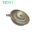
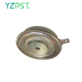
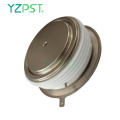
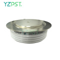
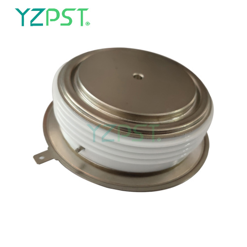
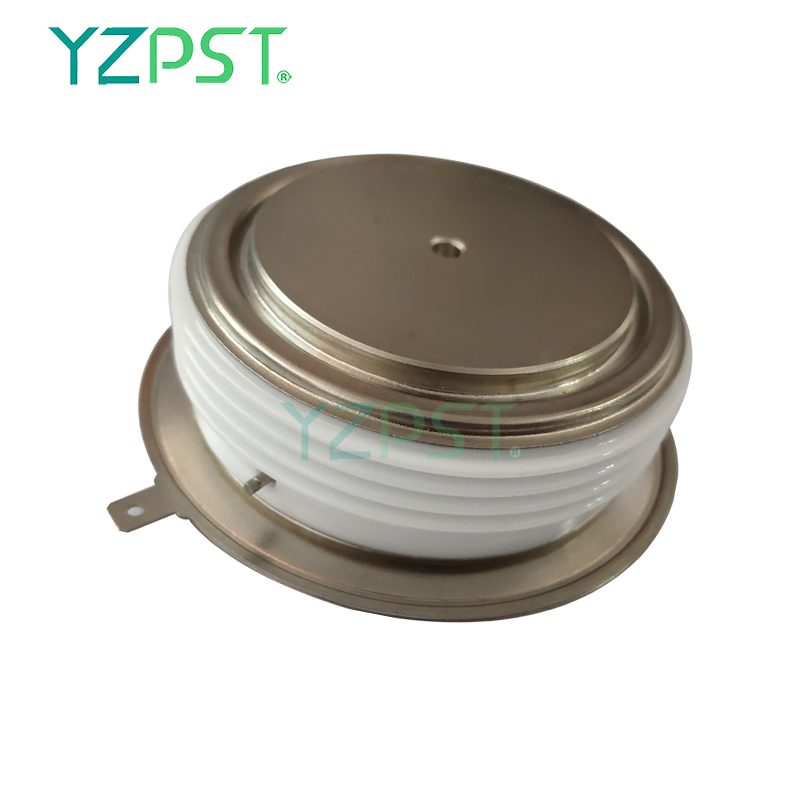
モデル: YZPST-R219CH12FN0
ブランド: YZPST
位相制御用の高電力サイリスタ
YZPST-R219CH12FN0
特徴:
保証最大ターンオフ時間
。すべての拡散構造
。圧力組立装置
インターデジタル増幅ゲート構成
。高いdV / dt機能
電気的特性と定格
ブロッキング-オフ状態
|
|
|
VRRM (1) |
VDRM (1) |
VRSM (1) |
|
1200 |
1200 |
1300 |
V RRM =繰り返しピーク逆電圧
V DRM =繰り返しピークオフ状態電圧
V RSM =非反復ピーク逆電圧(2)
|
Repetitive peak reverse leakage and off state leakage |
IRRM / IDRM |
15 mA 70 mA (3) |
|
Critical rate of voltage rise |
dV/dt (4) |
200 V/msec |
ノート:
特に指定がない限り、すべての定格はTj = 25 o Cに対して指定されています。
(1)すべての電圧定格は、適用される
上の50Hz / 60zHz正弦波
温度範囲-40〜+125 o C
(2)10ミリ秒最大パルス幅
(3)Tjの最大値= 125 o C
(4)80 V定格V DRMまでの線形および指数波形の最小値。ゲートが開いています。 Tj = 125 oC 。
(5)非反復値。
(6)di / dtの値は、 EIA / NIMA標準RS-397、セクション5-2-2-6を使用。定義された値 は、被試験スリスタと並列の 0.2 m Fコンデンサと20オームの抵抗で 構成される、低電圧回路から得られた値に追加さ れます。
実施中-状態
|
Parameter |
Symbol |
Min. |
Max. |
Typ. |
Units |
Conditions |
|
Max. average value of on-state current |
IT(AV)M |
|
929 |
|
A |
Sinewave,180o conduction,Tc=55oC |
|
RMS value of on-state current |
IT(RMS)m |
|
1893 |
|
A |
Nominal value |
|
Peak one cPSTCle surge (non repetitive) current |
ITSM |
|
-
9.0 |
|
kA
kA |
8.3 msec (60Hz), sinusoidal wave- shape, 180o conduction, Tj = 125 oC 10.0 msec (50Hz), sinusoidal wave- shape, 180o conduction, Tj = 125 oC |
|
I square t |
I2t |
|
405x103 |
|
A2s |
8.3 msec |
|
Latching current |
IL |
|
- |
|
mA |
VD = 24 V; RL= 12 ohms |
|
Holding current |
IH |
|
1000 |
|
mA |
VD = 24 V; I = 2.5 A |
|
Peak on-state voltage |
VTM |
|
2.04 |
|
V |
ITM = 1400 A |
|
Critical rate of rise of on-state current (5, 6) |
di/dt |
|
1500 |
|
A/ms |
Switching from VDRM £ 1000 V, non-repetitive |
|
Critical rate of rise of on-state current (6) |
di/dt |
|
1000 |
|
A/ms |
Switching from VDRM £ 1000 V |
ゲーティング
|
Parameter |
Symbol |
Min. |
Max. |
Typ. |
Units |
Conditions |
|
Peak gate power dissipation |
PGM |
|
30 |
|
W |
|
|
Average gate power dissipation |
PG(AV) |
|
2 |
|
W |
|
|
Peak gate current |
IGM |
|
- |
|
A |
|
|
Gate current required to trigger all units |
IGT |
|
300 |
|
mA |
VD = 10 V;IT=3A;Tj = +25 oC
|
|
Gate voltage required to trigger all units
|
VGT |
|
3.0 |
|
V
|
VD = 10 V;IT=3A;Tj = +25 oC
|
|
Peak negative voltage |
VRGM |
|
5 |
|
V |
|
動的
|
Parameter |
Symbol |
Min. |
Max. |
Typ. |
Units |
Conditions |
|
Delay time |
tgd |
|
1.0 |
- |
ms |
VD=67% VDRM, IT=2000A, di/dt=60A/us, IFG=2A, tr=0.5us, Tj=25C |
|
Turn-on time |
tgt |
|
2.0 |
- |
|
|
|
Turn-off time (with VR = -5 V) |
tq |
- |
- |
10 |
ms |
ITM=1000A, tp=1000us, di/dt=60A/us, Vr=50V, Vdr=33%VDRM, dVdr/dt=200V/us |
|
Reverse recovery current |
Irm |
|
- |
|
A |
ITM=4000A, tp=2000us, di/dt=60A/us |


電話番号: 86-514-87782298
Whatsapp: +8613805278321
住所: 3rd Floor, Weiheng Building No.20 B Area, Yangzhou, Jiangsu China
ウェブサイト: https://jp.yzpst.com


Privacy statement: Your privacy is very important to Us. Our company promises not to disclose your personal information to any external company with out your explicit permission.
Fill in more information so that we can get in touch with you faster
Privacy statement: Your privacy is very important to Us. Our company promises not to disclose your personal information to any external company with out your explicit permission.