

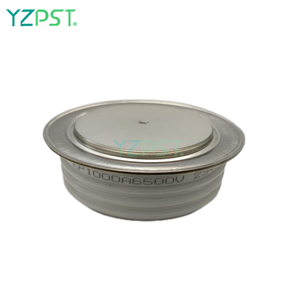
位相制御アプリケーション用の6500V高出力サイリスタ
$2502-9 Piece/Pieces
$210≥10Piece/Pieces
| お支払い方法の種類: | L/C,T/T,Paypal |
| インコタームズ: | FOB,CFR,CIF |
| 輸送方法: | Ocean,Land,Express,Others |
| ポート: | SHANGHAI |

$2502-9 Piece/Pieces
$210≥10Piece/Pieces
| お支払い方法の種類: | L/C,T/T,Paypal |
| インコタームズ: | FOB,CFR,CIF |
| 輸送方法: | Ocean,Land,Express,Others |
| ポート: | SHANGHAI |
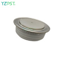
モデル: YZPST-KP1000A6500V
ブランド: yzpst
Place Of Origin: China
VRRM: 6500V
VDRM: 6500V
IRRM: 40 mA
IDRM: 200mA
DV/dt: 1000 V/μsec
IT(AV): 1000A
ITRMS: 1650A
| 販売単位 | : | Piece/Pieces |
| パッケージ型式 | : | 1.抗電気動態包装2.カートンボックス3.編組 |
| ダウンロード | : |
|
P/N:YZPST-KP1000A/6500V
高出力ティリストr 段階 コントロール アプリケーション
特徴:
。全て 拡散構造
。センター増幅GA TE構成
。保証されています 最大ターンオフ時間
。 高DV/DT 能力
。組み立てられた圧力 デバイス_

ブロッキング - オフステート
|
VRRM ( 1) |
V DRM ( 1) |
VRSM ( 1) |
|
6500 |
6500 |
6600 |
VRRM =繰り返しピーク逆電圧
VDRM =状態電圧オフオフの反復ピーク
VRSM =非反復ピーク逆電圧(2)
ノート:
すべての評価は、TJ = 25 ocに対して指定されています
それ以外の場合は述べられています。
(1)すべての電圧定格は、適用された50Hz/60ZHz正弦波波形に指定されています。
温度範囲-40〜 +125 oc。
(2)10ミリ秒。マックス。パルス幅
(3)TJ = 125 ocの最大値。
(4)線形および指数関数の最小値
80%の定格VDRMへの波状。ゲートが開いています。
TJ = 125 oc。
(5)非反復値。
(6)DI/DTの値はに確立されます
EIA/NIMA Standard RS-397、セクション5-2-2-6に従って。定義された値は、スリッサーと並行して0.2μFコンデンサと20オームの抵抗を含むスナバー回路から得られたものに加えて追加されます。
テスト中。
|
Repetitive peak reverse leakage and off state |
IRRM / IDRM |
40 mA 200mA (3) |
|
Critical rate of voltage rise |
dV/dt (4) |
1000 V/μsec |
指揮 - 状態
| Parameter | Symbol | Min. | Max. | Typ. | Units | Conditions |
| Max. Average value of on-state current | IT(AV) | 1000 | A | Sinewave, 180o conduction TC=70 oC | ||
| RMS value of on-state current | ITRMS | 1650 | A | Nominal value | ||
| Peak one cpstcle surge | ITSM | 18 | kA | 10.0 msec (50Hz), sinusoidal wave- shape, 180o conduction, Tj = 125 oC | ||
| (non repetitive) current | ||||||
| I square t | I2t | 1620 | kA2s | |||
| Latching current | IL | 1500 | mA | VD = 24 V; RL= 12 ohms | ||
| Holding current | IH | 500 | mA | VD = 24 V; I = 2.5 A | ||
| Peak on-state voltage | VTM | 2.65 | V | ITM = 1000A; Tvj= 125℃ | ||
| Threshold voltage | VTo | 1.24 | V | Tvj= 125℃ | ||
| Slope resistance | rT | 1.01 | mΩ | Tvj= 125℃ | ||
| Critical rate of rise of on-state current (5, 6) | di/dt | 500 | A/μs | Switching from VDRM < 1500 V, | ||
| non-repetitive | ||||||
| Critical rate of rise of on-state current (6) | di/dt | - | A/μs | Switching from VDRM < 3500 V |
|
Parameter |
Symbol |
Min. |
Max. |
Typ. |
Units |
Conditions |
|
Peak gate power dissipation |
PGM |
|
50 |
|
W |
tp = 40 us |
|
Average gate power dissipation |
PG(AV) |
|
10 |
|
W |
|
|
Peak gate current |
IGM |
|
10 |
|
A |
|
|
Gate current required to trigger all units |
IGT |
|
400 |
|
mA mA mA |
VD = 6 V;RL = 3 ohms;Tj = -40 oC VD = 6 V;RL = 3 ohms;Tj = +25 oC VD = 6 V;RL = 3 ohms;Tj = +125oC |
|
Gate voltage required to trigger all units |
VGT |
|
- 2.6 - |
|
V V V |
VD = 6 V;RL = 3 ohms;Tj = -40 oC VD = 6 V;RL = 3 ohms;Tj = 0- 125oC VD = Rated VDRM; RL = 1000 ohms; Tj = + 125 oC |
|
Peak negative voltage |
VGRM |
|
10 |
|
V |
|
動的
|
Parameter |
Symbol |
Min. |
Max. |
Typ. |
Units |
Conditions |
|
Delay time |
td |
|
- |
|
μs |
ITM = 1000 A; VD = Rated VDRM Gate pulse: VG = 20 V; RG = 20 ohms; tr = 0. 1 μs; tp = 20 μs |
|
Turn-off time (with VR = -50 V) |
tq |
|
700 |
|
μs |
ITM = 1000 A; di/dt = 1A/μs; VR > 200 V; Re-applied dV/dt = 20 V/μs linear to 67% VDRM; VG = 0; Tj = 125 oC; Duty cpstcle > 0.01% |
|
Reverse recovery charge |
Qrr |
|
- |
|
μAs |
ITM = 2000 A; di/dt = 1.5 A/μs; VR > 200V |
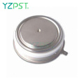
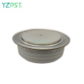
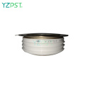
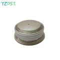
ケースアウトラインと 寸法。


電話番号: 86-514-87782298
Whatsapp: +8613805278321
住所: 3rd Floor, Weiheng Building No.20 B Area, Yangzhou, Jiangsu China
ウェブサイト: https://jp.yzpst.com


Privacy statement: Your privacy is very important to Us. Our company promises not to disclose your personal information to any external company with out your explicit permission.
Fill in more information so that we can get in touch with you faster
Privacy statement: Your privacy is very important to Us. Our company promises not to disclose your personal information to any external company with out your explicit permission.